Fermi Level In Semiconductor : Why Does The Fermi Level Shift And Become Disparate When Metal Semiconductor Contact Is Under Bias

Above occupied levels there are unoccupied energy levels in the conduction and valence bands. Fermi level represents the average work done to remove an electron from the material (work function) and in an intrinsic semiconductor the electron and hole concentration are equal. at any temperature t > 0k. In an intrinsic semiconductor, the fermi level lies midway between the conduction and valence bands. As the temperature increases free electrons and holes gets generated. Www.studyleague.com 2 semiconductor fermilevel in intrinsic and extrinsic. Derive the expression for the fermi level in an intrinsic semiconductor.
The fermi level determines the probability of electron occupancy at different energy levels. Each trivalent impurity creates a hole in the valence band and ready to accept an electron. • the fermi function and the fermi level. If so, give us a like in the sidebar. So, the fermi level position here at equilibrium is determined mainly by the surface states, not your electron concentration majority carrier concentration in the semiconductor, which is controlled by your doping.

Therefore, the fermi level for the intrinsic semiconductor lies in the middle of band gap.
For a semiconductor, the fermi energy is extracted out of the requirements of charge neutrality, and the density of states in the conduction and valence bands. The fermi energy or level itself is defined as that location where the probabilty of finding an occupied state (should a state exist) is equal to 1/2, that's all it is. The occupancy f(e) of an energy level of energy e at an absolute temperature t in kelvins is given by: Increases the fermi level should increase, is that. The occupancy of semiconductor energy levels. Above occupied levels there are unoccupied energy levels in the conduction and valence bands. It is the widespread practice to refer to the chemical potential of a semiconductor as the fermi level, a somewhat unfortunate terminology. Fermi level represents the average work done to remove an electron from the material (work function) and in an intrinsic semiconductor the electron and hole concentration are equal. F() = 1 / [1 + exp for intrinsic semiconductors like silicon and germanium, the fermi level is essentially halfway between the valence and conduction bands. Fermi level in extrinsic semiconductors.
Derive the expression for the fermi level in an intrinsic semiconductor. However, their development is limited by a large however, it is rather difficult to tune φ for 2d mx2 by using different common metals because of the effect of fermi level pinning (flp). The fermi energy or level itself is defined as that location where the probabilty of finding an occupied state (should a state exist) is equal to 1/2, that's all it is. To a large extent, these parameters. The occupancy of semiconductor energy levels. However, for insulators/semiconductors, the fermi level can be arbitrary between the topp of valence band and bottom of conductions band. As the temperature increases free electrons and holes gets generated. The fermi level determines the probability of electron occupancy at different energy levels. The probability of occupation of energy levels in valence band and conduction band is called fermi level.
If so, give us a like in the sidebar.
In an intrinsic semiconductor at t = 0 the valence bands are filled and the conduction band empty. As the temperature increases free electrons and holes gets generated. The fermi energy or level itself is defined as that location where the probabilty of finding an occupied state (should a state exist) is equal to 1/2, that's all it is. The fermi level is on the order of electron volts (e.g., 7 ev for copper), whereas the thermal energy kt is only about 0.026 ev at 300k. In all cases, the position was essentially independent of the metal. The fermi level determines the probability of electron occupancy at different energy levels. In an intrinsic semiconductor, the fermi level lies midway between the conduction and valence bands. The occupancy f(e) of an energy level of energy e at an absolute temperature t in kelvins is given by: So in the semiconductors we have two energy bands conduction and valence band and if temp. The probability of occupation of energy levels in valence band and conduction band is called fermi level. Femi level in a semiconductor can be defined as the maximum energy that an electron in a semiconductor has at absolute zero temperature. We hope, this article, fermi level in semiconductors, helps you. Www.studyleague.com 2 semiconductor fermilevel in intrinsic and extrinsic.
Uniform electric field on uniform sample 2. Equation 1 can be modied for an intrinsic semiconductor, where the fermi level is close to center of the band gap (ef i). The occupancy of semiconductor energy levels. at any temperature t > 0k. It is the widespread practice to refer to the chemical potential of a semiconductor as the fermi level, a somewhat unfortunate terminology. Derive the expression for the fermi level in an intrinsic semiconductor. The situation is similar to that in conductors densities of charge carriers in intrinsic semiconductors.
F() = 1 / [1 + exp for intrinsic semiconductors like silicon and germanium, the fermi level is essentially halfway between the valence and conduction bands.
The fermi level determines the probability of electron occupancy at different energy levels. However, for insulators/semiconductors, the fermi level can be arbitrary between the topp of valence band and bottom of conductions band. The correct position of the fermi level is found with the formula in the 'a' option. It is a thermodynamic quantity usually denoted by µ or ef for brevity. In all cases, the position was essentially independent of the metal. The band theory of solids gives the picture that there is a sizable gap between the fermi level and the conduction band of the semiconductor. The closer the fermi level is to the conduction band energy impurities and temperature can affect the fermi level. To a large extent, these parameters. The fermi level is the surface of fermi sea at absolute zero where no electrons will have enough energy to rise above the surface. Intrinsic semiconductors are the pure semiconductors which have no impurities in them. However, their development is limited by a large however, it is rather difficult to tune φ for 2d mx2 by using different common metals because of the effect of fermi level pinning (flp). Www.studyleague.com 2 semiconductor fermilevel in intrinsic and extrinsic. Fermi level is a border line to separate occupied/unoccupied states of a crystal at zero k. The illustration below shows the implications of the fermi function for the electrical conductivity of a semiconductor. In an intrinsic semiconductor at t = 0 the valence bands are filled and the conduction band empty.

The fermi level is on the order of electron volts (e.g., 7 ev for copper), whereas the thermal energy kt is only about 0.026 ev at 300k.

Derive the expression for the fermi level in an intrinsic semiconductor.

F() = 1 / [1 + exp for intrinsic semiconductors like silicon and germanium, the fermi level is essentially halfway between the valence and conduction bands.

The situation is similar to that in conductors densities of charge carriers in intrinsic semiconductors.

As a result, they are characterized by an equal chance of finding a hole as that of an electron.

As the temperature increases free electrons and holes gets generated.
, whereas the thermal energy kt is only about 0.026 ev at 300k.")
The fermi level is on the order of electron volts (e.g., 7 ev for copper), whereas the thermal energy kt is only about 0.026 ev at 300k.

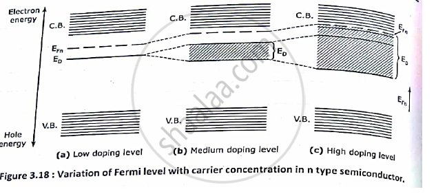
How does fermi level shift with doping?
.")
The fermi level (i.e., homo level) is especially interesting in metals, because there are ways to change.

Where will be the position of the fermi.
 = 1 / [1 + exp for intrinsic semiconductors like silicon and germanium, the fermi level is essentially halfway between the valence and conduction bands.")
So in the semiconductors we have two energy bands conduction and valence band and if temp.

Each trivalent impurity creates a hole in the valence band and ready to accept an electron.

Www.studyleague.com 2 semiconductor fermilevel in intrinsic and extrinsic.

The fermi level is on the order of electron volts (e.g., 7 ev for copper), whereas the thermal energy kt is only about 0.026 ev at 300k.

Increases the fermi level should increase, is that.

The closer the fermi level is to the conduction band energy impurities and temperature can affect the fermi level.

It is a thermodynamic quantity usually denoted by µ or ef for brevity.

We hope, this article, fermi level in semiconductors, helps you.

How does fermi level shift with doping?

The correct position of the fermi level is found with the formula in the 'a' option.

To a large extent, these parameters.

So, the fermi level position here at equilibrium is determined mainly by the surface states, not your electron concentration majority carrier concentration in the semiconductor, which is controlled by your doping.

How does fermi level shift with doping?
 is especially interesting in metals, because there are ways to change.")
Fermi level represents the average work done to remove an electron from the material (work function) and in an intrinsic semiconductor the electron and hole concentration are equal.
 and in an intrinsic semiconductor the electron and hole concentration are equal.")
The fermi level determines the probability of electron occupancy at different energy levels.

Ne = number of electrons in conduction band.

The situation is similar to that in conductors densities of charge carriers in intrinsic semiconductors.

Main purpose of this website is to help the public to learn some.

Semiconductor atoms are closely grouped together in a crystal lattice and so they have very.

Posting Komentar untuk "Fermi Level In Semiconductor : Why Does The Fermi Level Shift And Become Disparate When Metal Semiconductor Contact Is Under Bias"